
LEARN ABOUT NANO TECHNOLOGY
EDUCATION
Are you looking for nano & micro technology program that fits your school needs?
Discover NowLEARN ABOUT US
PRODUCTS
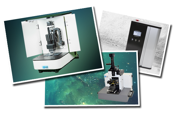
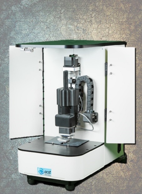
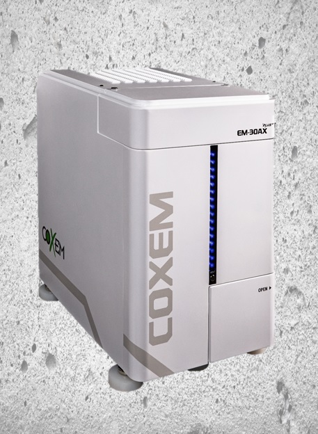
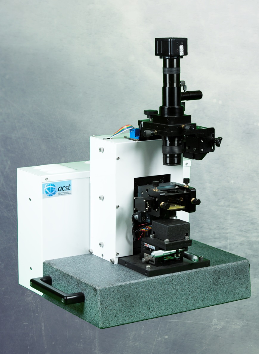
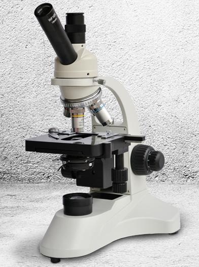
Explore our wide range of products metrology, microscopy and lithography tools.
DETAILSWIDE VARIETY OF CONSUMABLES
SHOP ONLINE
AFM Probes, Substrates, micro-Reservoirs, accessories, imaging processing software and more.
SHOP HERE